June 07, 2011

RF based REMOTE CONTROL

Introduction:-
                  The rf transmitter a gadget that disseminates radio waves with the help of an antenna. A rf transmitter consists of an oscillator that changes electrical power in to a reasonable frequency. There is also an amplifier for audio frequency (AF) and radio frequency (RF). A modulator regulates the signal information on to the transmitter for dispersion. The rf transmitter has an important component that makes its working possible; this is the antenna that transmits an electromagnetic signal for many types of communication. rf transmitter works together with rf receivers. There must be rf receivers on the other end for transmitters to play their role. Communication by use of these systems is possible for radios, cell phones, televisions, walkie –talkies and other electronics used for the purpose of broadcasting. It is possible to find both rf receivers and transmitters in one device. A good example of such technology is used in mobile phones where one can receive and call using one gadget. Currently communication does not rely on analogue mode but uses digital technology thus eliminating the need for complex wiring system to do the connections that carry information.
For an example: We will be using ASK (Amplitude Shift Keying) based Tx/Rx(transmitter/receiver) pair operating at 433 MHz. The transmitter module accepts serial data at a maximum of XX baud rate. It can be directly interfaced with a microcontroller or can be used in remote control applications with the help of encoder/decoder ICs.


RF transmitter module:-


RF transmitter module


RF receiver module:-


RF Receiver module


Working:-

The encoder IC takes in parallel data which is to be transmitted, packages it into serial format and then transmits it with the help of the RF transmitter module. At the receiver end the decoder IC receives the signal via the RF receiver module, decodes the serial data and reproduces the original data in the parallel format.In order to control say a dc motor, we require 2 bits of information (switching it on/off) while we need 4 bits of information to control 2 motors. HT12E and HT12D are 4 channel encoder/decoder ICs directly compatible with the specified RF module.In order to drive motors, we would need to connect a suitable motor driver at the output of the decoder IC. The motor driver circuit can consist of a relay, transistorized H-Bridge or motor driver ICs like the L293D, L298 etc. 


Block Diagram:-


Application:-


                 Rf transmitter enables you to make use of your television, radio, phone and other communication hand held devices. Rf receivers are installed in these devices in factory to make them respond to any signal send. A rf transmitter may interfere with other communication services. This means that you should take precaution by seeking from the relevant authorities about the mode of frequency to use when installing your communication system. Rf receivers are capable of receiving broadcast information from a rf transmitter in different patterns like a single beam or broadcast system. You cannot however tell the difference when you are listening from your radio or watching TV. Rf receivers function hand by hand with transmitters so none can be on its own. Communication is hence a two-way traffic and some communication models are accommodating the receiving and transmitting factors in one equipment. These functions perform well by the energy from electricity or solar. The major important thing in a communication system is to send and receive feedback. Modern times have included the aspect of time in the instruments of passing information no matter how far you are located. This would however be impossible if it was not for transmitters and receivers.


June 06, 2011

What is RFID
 
RFID stands for Radio-Frequency IDentification. The acronym refers to small electronic devices that consist of a small chip and an antenna. The chip typically is capable of carrying 2,000 bytes of data or less.
The RFID device serves the same purpose as a bar code or a magnetic strip on the back of a credit card or ATM card; it provides a unique identifier for that object. And, just as a bar code or magnetic strip must be scanned to get the information, the RFID device must be scanned to retrieve the identifying information. 

Working

A Radio-Frequency IDentification system has three parts:
  • A scanning antenna
  • A transceiver with a decoder to interpret the data
  • A transponder - the RFID tag - that has been programmed with information.
The scanning antenna puts out radio-frequency signals in a relatively short range. The RF radiation does two things:
  • It provides a means of communicating with the transponder (the RFID tag) AND
  • It provides the RFID tag with the energy to communicate (in the case of passive RFID tags).
This is an absolutely key part of the technology; RFID tags do not need to contain batteries, and can therefore remain usable for very long periods of time (maybe decades). The scanning antennas can be permanently affixed to a surface; handheld antennas are also available. They can take whatever shape you need; for example, you could build them into a door frame to accept data from persons or objects passing through.
When an RFID tag passes through the field of the scanning antenna, it detects the activation signal from the antenna. That "wakes up" the RFID chip, and it transmits the information on its microchip to be picked up by the scanning antenna.


In addition, the RFID tag may be of one of two types. Active RFID tags have their own power source; the advantage of these tags is that the reader can be much farther away and still get the signal. Even though some of these devices are built to have up to a 10 year life span, they have limited life spans. Passive RFID tags, however, do not require batteries, and can be much smaller and have a virtually unlimited life span.
RFID tags can be read in a wide variety of circumstances, where barcodes or other optically read technologies are useless.
  • The tag need not be on the surface of the object (and is therefore not subject to wear)
  • The read time is typically less than 100 milliseconds
  • Large numbers of tags can be read at once rather than item by item. 

Passive RFID vs. Active RFID

Passive RFID tags operate using power from the RFID transceiver. Passive tags are small and inexpensive, but do not have good range.
Active RFID tags are powered, usually by a battery. Active tags are larger and more expensive, but offer a much better identification range.
RFID tags store data, which is typically used for authentication. Passive tags typically store between 32 and 128 bits of data; Active tags can store up to 1MB of data.
Passive tags are Read-Only; Active tags are typically rewritable.

Applications

Please click at one of the applications below to read how Rotil Communications B.V. applied these techniques successfully at previous projects.
  • Vehicle start interruption
  • Access control and identification
  • Petrol stations
  • Working hours registration system
Other possibilities to apply the RFID technique are for example:

Vehicle identification

Every vehicle will carry a transponder. Through the unique id number in the transponder it will be easy to ‘recognise’ the vehicle. This can expanded with the registration of technical vehicle information such as temperature, GPS location.

Logistic processes

Every container, box or crate has a transponder fitted to it. With each step in the process, the transponder is being read and the operation is saved in the central database. By this is, it will be very easy to find out which steps in the production process has already been made.

Service and maintenance

All products, devices or vehicles will get a transponder. The service or maintenance mechanic scans this transponder for each maintenance. The software on a computer, which is connected to a central database, enables him to register for example the product details, customer number, maintenance tasks, date/time. Now it will be much easier to find out which maintenance or service has been provided to a certain product/vehicle with just a click. This will be very (cost) efficient.

October 10, 2009

Countdown Timer using 555 Timer

Countdown Timer:-
In this Countdown Timer project, a 555 IC, a counter IC and a transistor switch to activate a relay either ON/OFF (mode selected by a jumper) as soon as the counting period is over. The circuit consists of an oscillator, a ripple and two switching transistors.

Oscillator:-
The 555 is configured in the standard astable oscillator circuit designed to give a square wave cycle at a period of around 1 cycle/sec. A potentiometer is included in the design so the period can be set to exactly 1 second by timing the LED flashes. A jumper connection is provided so the LED can be turned off. As soon as power is applied to the circuit counting begins. The output pulse from pin 3 of the 555 is fed to a the clock input pin 10 of the 14-stage binary ripple counter, the 4020 (or 14020.).

parts required:-


Circuitdiagram:-

http://img238.imageshack.us/img238/1066/cntdntmrfig1a.gif

Ripple Counter:-

The counter output wanted is set by a jumper. Ten counter outputs are available: 8/16/32/64/128/256/512/1024/4096 and 8192 counts. If the 555 is set to oscillate at exactly 1.0Hz by the on-board trimpot then the maximum timer interval which can be set is 8192 seconds (just over 2 hours.) At the end of the counting of the countdown timer period a pulse is output on the pin with the jumper on it. The 14020 ripple counter advances its count on each negative transistion of the clock pulse from the 555. So for each output cycle of low-high-low-high the count is advanced by two. It can be set to an zero state (all outputs low) by a logic high applied to pin 11.

In this circuit C3, R4 and D1 are arranged as a power-on reset. When power is applied to the circuit C3 is in a discharged state so pin 11 will be pulled high. C3 will quickly charge via R4 and the level at pin 11 falls thus enabling the counter. The 14020 then counts clock pulses until the selected counter output goes high. D1 provides a discharge path for C3 when the power is disconnected.

You can change the components values of R1 and C1 to set the 555 count frequency to more than 1.0 Hz. If you change the count to 10 seconds then a maximum timer delay of 81920 seconds, or 22.7 hours, can be obtained.

Transistors:-

The output from the 4020 goes to a transistor switch arrangement. Two BC547 are connected so that either switching option for the relay is available. A jumper sets the option. The relay can turn ON when power and counting start then turn OFF after the count period, or it can do the opposite. The relay will turn ON after the end of the count period and stay on so long as power is supplied to the circuit. Note that the reset pin of the 555 is connected to the collector of Q1. This enables the 555 during the counting as the collector of Q1 is pulled low.


September 27, 2009

MOSFET

Introduction:-

The metal–oxide–semiconductor field-effect transistor (MOSFET, MOS-FET, or MOS FET) is a device used to amplify or switch electronic signals. The basic principle of the device was first proposed by Julius Edgar Lilienfeld in 1925. The MOSFET includes a channel of n-type or p-type semiconductor material (see article on semiconductor devices), and is accordingly called an NMOSFET or a PMOSFET (also commonly nMOS, pMOS). It is by far the most common transistor in both digital and analog circuits, though the bipolar junction transistorwas at one time much more common.

Diagramatic representation...


http://img198.imageshack.us/img198/7159/mosfet.jpg

Circuit symbol:-

http://img5.imageshack.us/img5/6906/schematicsymbolsmosfet.png

MOSFET operation:-

A traditional metal–oxide–semiconductor (MOS) structure is obtained by growing a layer of silicon dioxide (SiO2) on top of a silicon substrate and depositing a layer of metal or polycrystalline silicon (the latter is commonly used). As the silicon dioxide is a dielectric material, its structure is equivalent to a planar capacitor, with one of the electrodes replaced by a semiconductor.

When a voltage is applied across a MOS structure, it modifies the distribution of charges in the semiconductor. If we consider a P-type semiconductor (with NA the density of acceptors, p the density of holes; p = NA in neutral bulk), a positive voltage, VGB, from gate to body (see figure) creates a depletion layer by forcing the positively charged holes away from the gate-insulator/semiconductor interface, leaving exposed a carrier-free region of immobile, negatively charged acceptor ions (see doping (semiconductor)). If VGB is high enough, a high concentration of negative charge carriers forms in an inversion layer located in a thin layer next to the interface between the semiconductor and the insulator. Unlike the MOSFET, where the inversion layer electrons are supplied rapidly from the source/drain electrodes, in the MOS capacitor they are produced much more slowly by thermal generation through carrier generation and recombination centers in the depletion region. Conventionally, the gate voltage at which the volume density of electrons in the inversion layer is the same as the volume density of holes in the body is called the threshold voltage.

This structure with P-type body is the basis of the N-type MOSFET, which requires the addition of an N-type source and drain regions.

Modes of operation

The operation of a MOSFET can be separated into three different modes, depending on the voltages at the terminals. In the following discussion, a simplified algebraic model is used that is accurate only for old technology. Modern MOSFET characteristics require computer models that have rather more complex behavior. For example, see Liu and the device modeling list at Designers-guide.org.

For an enhancement-mode, n-channel MOSFET, the three operational modes are:

Cutoff, subthreshold, or weak-inversion mode When VGS <>th: where Vth is the threshold voltage of the device. According to the basic threshold model, the transistor is turned off, and there is no conduction between drain and source. In reality, the Boltzmann distribution of electron energies allows some of the more energetic electrons at the source to enter the channel and flow to the drain, resulting in a subthreshold current that is an exponential function of gate–source voltage. While the current between drain and source should ideally be zero when the transistor is being used as a turned-off switch, there is a weak-inversion current, sometimes called subthreshold leakage.In weak inversion the current varies exponentially with gate-to-source bias VGS as given approximately by:
http://img10.imageshack.us/img10/7092/5b9727f63fc863196c6f4e0.png

, where ID0 = current at VGS = Vth and the slope factor n is given by n = 1 + CD / COX, with CD = capacitance of the depletion layer and COX = capacitance of the oxide layer. In a long-channel device, there is no drain voltage dependence of the current once VDS > > VT, but as channel length is reduced drain-induced barrier lowering introduces drain voltage dependence that depends in a complex way upon the device geometry (for example, the channel doping, the junction doping and so on). Frequently, threshold voltage Vth for this mode is defined as the gate voltage at which a selected value of current ID0 occurs, for example, ID0 = 1 μA, which may not be the same Vth-value used in the equations for the following modes. Some micropower analog circuits are designed to take advantage of subthreshold conduction. By working in the weak-inversion region, the MOSFETs in these circuits deliver the highest possible transconductance-to-current ratio, namely: gm / ID = 1 / (nVT), almost that of a bipolar transistor. The subthreshold I-V relation depends exponentially upon threshold voltage, introducing a strong dependence on any manufacturing variation that affects threshold voltage; for example: variations in oxide thickness, junction depth, or body doping that change the degree of drain-induced barrier lowering. The resulting sensitivity to fabricational variations complicates optimization of circuits operating in the subthreshold mode.

Triode mode or linear region (also known as the ohmic mode)
When VGS > Vth and VDS < ( VGS - Vth )
The transistor is turned on, and a channel has been created which allows current to flow between the drain and the source. The MOSFET operates like a resistor, controlled by the gate voltage relative to both the source and drain voltages. The current from drain to source is modeled as:

http://img30.imageshack.us/img30/1988/a713a6eb38e5a4f0531a014.png
where μn is the charge-carrier effective mobility, W is the gate width, L is the gate length and Cox is the gate oxide capacitance per unit area. The transition from the exponential subthreshold region to the triode region is not as sharp as the equations suggest.
Saturation or active mode

When VGS > Vth and VDS > ( VGS - Vth )The switch is turned on, and a channel has been created, which allows current to flow between the drain and source. Since the drain voltage is higher than the gate voltage, the electrons spread out, and conduction is not through a narrow channel but through a broader, two- or three-dimensional current distribution extending away from the interface and deeper in the substrate. The onset of this region is also known as pinch-off to indicate the lack of channel region near the drain. The drain current is now weakly dependent upon drain voltage and controlled primarily by the gate–source voltage, and modeled very approximately as:

http://img132.imageshack.us/img132/1897/ea8ecd051837b6b88bd5036.png
The additional factor involving λ, the channel-length modulation parameter, models current dependence on drain voltage due to the Early effect, or channel length modulation. According to this equation, a key design parameter, the MOSFET transconductance is:
http://img15.imageshack.us/img15/864/4ffd9e4240ecc5b95c4bf7f.png, where the combination Vov = VGS - Vth is called the overdrive voltage. Another key design parameter is the MOSFET output resistance rO given by:
http://img15.imageshack.us/img15/1252/5b150eff3803082f6585ffd.png
. If λ is taken as zero, an infinite output resistance of the device results that leads to unrealistic circuit predictions, particularly in analog circuits.As the channel length becomes very short, these equations become quite inaccurate. New physical effects arise. For example, carrier transport in the active mode may become limited by velocity saturation. When velocity saturation dominates, the saturation drain current is more nearly linear than quadratic in VGS. At even shorter lengths, carriers transport with near zero scattering, known as quasi-ballistic transport. In addition, the output current is affected by drain-induced barrier lowering of the threshold voltage.

September 21, 2009

JFET

INTRODUCTION:-

The junction gate field-effect transistor (JFET or JUGFET) is the simplest type of field effect transister. It can be used as an electrically-controlled switch or as a voltage-controlled resistance . electric charge flowflows through a semiconducting channel between "source" and "drain" terminals. By applying a bias voltage to a "gate" terminal, the channel is "pinched", so that the electric current is impeded or switched off completely.

Structure:-

The JFET is a long channel of semiconductor material, doped to contain an abundance of positive charge carriers (p-type), or of negative carriers (n-type). Contacts at each end form the source and drain. The gate (control) terminal has doping opposite to that of the channel, which it surrounds, so that there is a P-N junction at the interface. Terminals to connect with the outside are usually made ohmic.

Function:-

JFET operation is like that of a garden hose. The flow of water through a hose can be controlled by squeezing it to reduce the cross section; the flow of electric charge through a JFET is controlled by constricting the current-carrying channel. The current depends also on the electric field between source and drain.

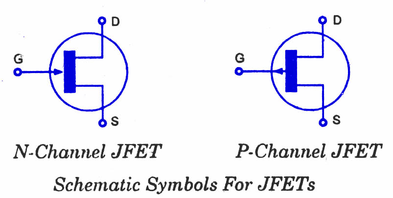
Symbols:-


The JFET gate is sometimes drawn in the middle of the channel (instead of at the drain or source electrode as in these examples). This symmetry suggests that "drain" and "source" are interchangeable, so the symbol should be used only for those JFETs where they are indeed interchangeable (which is not true of all JFETs).

Officially, the style of the symbol should show the component inside a circle (representing the envelope of a discrete device). This is true in both the US and Europe. The symbol is usually drawn without the circle when drawing schematics of integrated circuits. More recently, the symbol is often drawn without its circle even for discrete devices.

COMMON COLLECTOR CONFIGURATION

INTRODUCTION:-

The COMMON-COLLECTOR CONFIGURATION (CC) is used as a current driver for
impedance matching and is particularly useful in switching circuits. The CC is also referred to as an
emitter-follower and is equivalent to the electron-tube cathode follower. Both have high input impedance
and low output impedance.In the CC, the input is applied to the base, the output is taken from the emitter, and the collector is
the element common to both input and output.

Circuit diagram:-

Gain:-

GAIN is a term used to describe the amplification capabilities of an amplifier. It is basically a ratio
of output to input. The current gain for the three transistor configurations (CB, CE, and CC) are ALPHA
(a), BETA (b), and GAMMA (g), respectively

formula:-


Purpose:-
The TRANSISTOR CONFIGURATION COMPARISON CHART gives a rundown of the
different properties of the three configurations.

COMMON BASE CONFIGURATION

Introduction:-

The COMMON-EMITTER CONFIGURATION (CE) is the most frequently used configuration
in practical amplifier circuits, since it provides good voltage, current, and power gain. The input to the CE
is applied to the base-emitter circuit and the output is taken from the collector-emitter circuit, making the
emitter the element "common" to both input and output. The CE is set apart from the other configurations,
because it is the only configuration that provides a phase reversal between input and output signals.

Circuit diagram:-


Purpose:-

The COMMON-BASE CONFIGURATION (CB) is mainly used for impedance matching, since it
has a low input resistance and a high output resistance. It also has a current gain of less than
In the CB, the input is applied to the emitter, the output is taken from the collector, and the base is
the element common to both input and output.

DOOR BELL FOR DEAF CLICK HERE

Electronics is the study and use of electrical that operate by controlling the flow of electrons or other electrically charged particles in devices such as thermionic valves. and semiconductors. The pure study of such devices is considered as a branch of physics, while the design and construction electronic circuits to solve practical problems is called electronic engineering.

Popular article