October 10, 2009

Countdown Timer using 555 Timer

Countdown Timer:-
In this Countdown Timer project, a 555 IC, a counter IC and a transistor switch to activate a relay either ON/OFF (mode selected by a jumper) as soon as the counting period is over. The circuit consists of an oscillator, a ripple and two switching transistors.

Oscillator:-
The 555 is configured in the standard astable oscillator circuit designed to give a square wave cycle at a period of around 1 cycle/sec. A potentiometer is included in the design so the period can be set to exactly 1 second by timing the LED flashes. A jumper connection is provided so the LED can be turned off. As soon as power is applied to the circuit counting begins. The output pulse from pin 3 of the 555 is fed to a the clock input pin 10 of the 14-stage binary ripple counter, the 4020 (or 14020.).

parts required:-


Circuitdiagram:-

http://img238.imageshack.us/img238/1066/cntdntmrfig1a.gif

Ripple Counter:-

The counter output wanted is set by a jumper. Ten counter outputs are available: 8/16/32/64/128/256/512/1024/4096 and 8192 counts. If the 555 is set to oscillate at exactly 1.0Hz by the on-board trimpot then the maximum timer interval which can be set is 8192 seconds (just over 2 hours.) At the end of the counting of the countdown timer period a pulse is output on the pin with the jumper on it. The 14020 ripple counter advances its count on each negative transistion of the clock pulse from the 555. So for each output cycle of low-high-low-high the count is advanced by two. It can be set to an zero state (all outputs low) by a logic high applied to pin 11.

In this circuit C3, R4 and D1 are arranged as a power-on reset. When power is applied to the circuit C3 is in a discharged state so pin 11 will be pulled high. C3 will quickly charge via R4 and the level at pin 11 falls thus enabling the counter. The 14020 then counts clock pulses until the selected counter output goes high. D1 provides a discharge path for C3 when the power is disconnected.

You can change the components values of R1 and C1 to set the 555 count frequency to more than 1.0 Hz. If you change the count to 10 seconds then a maximum timer delay of 81920 seconds, or 22.7 hours, can be obtained.

Transistors:-

The output from the 4020 goes to a transistor switch arrangement. Two BC547 are connected so that either switching option for the relay is available. A jumper sets the option. The relay can turn ON when power and counting start then turn OFF after the count period, or it can do the opposite. The relay will turn ON after the end of the count period and stay on so long as power is supplied to the circuit. Note that the reset pin of the 555 is connected to the collector of Q1. This enables the 555 during the counting as the collector of Q1 is pulled low.


September 27, 2009

MOSFET

Introduction:-

The metal–oxide–semiconductor field-effect transistor (MOSFET, MOS-FET, or MOS FET) is a device used to amplify or switch electronic signals. The basic principle of the device was first proposed by Julius Edgar Lilienfeld in 1925. The MOSFET includes a channel of n-type or p-type semiconductor material (see article on semiconductor devices), and is accordingly called an NMOSFET or a PMOSFET (also commonly nMOS, pMOS). It is by far the most common transistor in both digital and analog circuits, though the bipolar junction transistorwas at one time much more common.

Diagramatic representation...


http://img198.imageshack.us/img198/7159/mosfet.jpg

Circuit symbol:-

http://img5.imageshack.us/img5/6906/schematicsymbolsmosfet.png

MOSFET operation:-

A traditional metal–oxide–semiconductor (MOS) structure is obtained by growing a layer of silicon dioxide (SiO2) on top of a silicon substrate and depositing a layer of metal or polycrystalline silicon (the latter is commonly used). As the silicon dioxide is a dielectric material, its structure is equivalent to a planar capacitor, with one of the electrodes replaced by a semiconductor.

When a voltage is applied across a MOS structure, it modifies the distribution of charges in the semiconductor. If we consider a P-type semiconductor (with NA the density of acceptors, p the density of holes; p = NA in neutral bulk), a positive voltage, VGB, from gate to body (see figure) creates a depletion layer by forcing the positively charged holes away from the gate-insulator/semiconductor interface, leaving exposed a carrier-free region of immobile, negatively charged acceptor ions (see doping (semiconductor)). If VGB is high enough, a high concentration of negative charge carriers forms in an inversion layer located in a thin layer next to the interface between the semiconductor and the insulator. Unlike the MOSFET, where the inversion layer electrons are supplied rapidly from the source/drain electrodes, in the MOS capacitor they are produced much more slowly by thermal generation through carrier generation and recombination centers in the depletion region. Conventionally, the gate voltage at which the volume density of electrons in the inversion layer is the same as the volume density of holes in the body is called the threshold voltage.

This structure with P-type body is the basis of the N-type MOSFET, which requires the addition of an N-type source and drain regions.

Modes of operation

The operation of a MOSFET can be separated into three different modes, depending on the voltages at the terminals. In the following discussion, a simplified algebraic model is used that is accurate only for old technology. Modern MOSFET characteristics require computer models that have rather more complex behavior. For example, see Liu and the device modeling list at Designers-guide.org.

For an enhancement-mode, n-channel MOSFET, the three operational modes are:

Cutoff, subthreshold, or weak-inversion mode When VGS <>th: where Vth is the threshold voltage of the device. According to the basic threshold model, the transistor is turned off, and there is no conduction between drain and source. In reality, the Boltzmann distribution of electron energies allows some of the more energetic electrons at the source to enter the channel and flow to the drain, resulting in a subthreshold current that is an exponential function of gate–source voltage. While the current between drain and source should ideally be zero when the transistor is being used as a turned-off switch, there is a weak-inversion current, sometimes called subthreshold leakage.In weak inversion the current varies exponentially with gate-to-source bias VGS as given approximately by:
http://img10.imageshack.us/img10/7092/5b9727f63fc863196c6f4e0.png

, where ID0 = current at VGS = Vth and the slope factor n is given by n = 1 + CD / COX, with CD = capacitance of the depletion layer and COX = capacitance of the oxide layer. In a long-channel device, there is no drain voltage dependence of the current once VDS > > VT, but as channel length is reduced drain-induced barrier lowering introduces drain voltage dependence that depends in a complex way upon the device geometry (for example, the channel doping, the junction doping and so on). Frequently, threshold voltage Vth for this mode is defined as the gate voltage at which a selected value of current ID0 occurs, for example, ID0 = 1 μA, which may not be the same Vth-value used in the equations for the following modes. Some micropower analog circuits are designed to take advantage of subthreshold conduction. By working in the weak-inversion region, the MOSFETs in these circuits deliver the highest possible transconductance-to-current ratio, namely: gm / ID = 1 / (nVT), almost that of a bipolar transistor. The subthreshold I-V relation depends exponentially upon threshold voltage, introducing a strong dependence on any manufacturing variation that affects threshold voltage; for example: variations in oxide thickness, junction depth, or body doping that change the degree of drain-induced barrier lowering. The resulting sensitivity to fabricational variations complicates optimization of circuits operating in the subthreshold mode.

Triode mode or linear region (also known as the ohmic mode)
When VGS > Vth and VDS < ( VGS - Vth )
The transistor is turned on, and a channel has been created which allows current to flow between the drain and the source. The MOSFET operates like a resistor, controlled by the gate voltage relative to both the source and drain voltages. The current from drain to source is modeled as:

http://img30.imageshack.us/img30/1988/a713a6eb38e5a4f0531a014.png
where μn is the charge-carrier effective mobility, W is the gate width, L is the gate length and Cox is the gate oxide capacitance per unit area. The transition from the exponential subthreshold region to the triode region is not as sharp as the equations suggest.
Saturation or active mode

When VGS > Vth and VDS > ( VGS - Vth )The switch is turned on, and a channel has been created, which allows current to flow between the drain and source. Since the drain voltage is higher than the gate voltage, the electrons spread out, and conduction is not through a narrow channel but through a broader, two- or three-dimensional current distribution extending away from the interface and deeper in the substrate. The onset of this region is also known as pinch-off to indicate the lack of channel region near the drain. The drain current is now weakly dependent upon drain voltage and controlled primarily by the gate–source voltage, and modeled very approximately as:

http://img132.imageshack.us/img132/1897/ea8ecd051837b6b88bd5036.png
The additional factor involving λ, the channel-length modulation parameter, models current dependence on drain voltage due to the Early effect, or channel length modulation. According to this equation, a key design parameter, the MOSFET transconductance is:
http://img15.imageshack.us/img15/864/4ffd9e4240ecc5b95c4bf7f.png, where the combination Vov = VGS - Vth is called the overdrive voltage. Another key design parameter is the MOSFET output resistance rO given by:
http://img15.imageshack.us/img15/1252/5b150eff3803082f6585ffd.png
. If λ is taken as zero, an infinite output resistance of the device results that leads to unrealistic circuit predictions, particularly in analog circuits.As the channel length becomes very short, these equations become quite inaccurate. New physical effects arise. For example, carrier transport in the active mode may become limited by velocity saturation. When velocity saturation dominates, the saturation drain current is more nearly linear than quadratic in VGS. At even shorter lengths, carriers transport with near zero scattering, known as quasi-ballistic transport. In addition, the output current is affected by drain-induced barrier lowering of the threshold voltage.

September 21, 2009

JFET

INTRODUCTION:-

The junction gate field-effect transistor (JFET or JUGFET) is the simplest type of field effect transister. It can be used as an electrically-controlled switch or as a voltage-controlled resistance . electric charge flowflows through a semiconducting channel between "source" and "drain" terminals. By applying a bias voltage to a "gate" terminal, the channel is "pinched", so that the electric current is impeded or switched off completely.

Structure:-

The JFET is a long channel of semiconductor material, doped to contain an abundance of positive charge carriers (p-type), or of negative carriers (n-type). Contacts at each end form the source and drain. The gate (control) terminal has doping opposite to that of the channel, which it surrounds, so that there is a P-N junction at the interface. Terminals to connect with the outside are usually made ohmic.

Function:-

JFET operation is like that of a garden hose. The flow of water through a hose can be controlled by squeezing it to reduce the cross section; the flow of electric charge through a JFET is controlled by constricting the current-carrying channel. The current depends also on the electric field between source and drain.

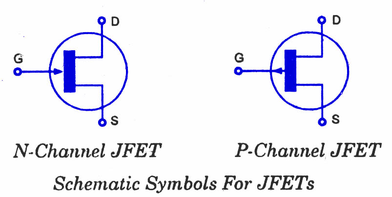
Symbols:-


The JFET gate is sometimes drawn in the middle of the channel (instead of at the drain or source electrode as in these examples). This symmetry suggests that "drain" and "source" are interchangeable, so the symbol should be used only for those JFETs where they are indeed interchangeable (which is not true of all JFETs).

Officially, the style of the symbol should show the component inside a circle (representing the envelope of a discrete device). This is true in both the US and Europe. The symbol is usually drawn without the circle when drawing schematics of integrated circuits. More recently, the symbol is often drawn without its circle even for discrete devices.

COMMON COLLECTOR CONFIGURATION

INTRODUCTION:-

The COMMON-COLLECTOR CONFIGURATION (CC) is used as a current driver for
impedance matching and is particularly useful in switching circuits. The CC is also referred to as an
emitter-follower and is equivalent to the electron-tube cathode follower. Both have high input impedance
and low output impedance.In the CC, the input is applied to the base, the output is taken from the emitter, and the collector is
the element common to both input and output.

Circuit diagram:-

Gain:-

GAIN is a term used to describe the amplification capabilities of an amplifier. It is basically a ratio
of output to input. The current gain for the three transistor configurations (CB, CE, and CC) are ALPHA
(a), BETA (b), and GAMMA (g), respectively

formula:-


Purpose:-
The TRANSISTOR CONFIGURATION COMPARISON CHART gives a rundown of the
different properties of the three configurations.

COMMON BASE CONFIGURATION

Introduction:-

The COMMON-EMITTER CONFIGURATION (CE) is the most frequently used configuration
in practical amplifier circuits, since it provides good voltage, current, and power gain. The input to the CE
is applied to the base-emitter circuit and the output is taken from the collector-emitter circuit, making the
emitter the element "common" to both input and output. The CE is set apart from the other configurations,
because it is the only configuration that provides a phase reversal between input and output signals.

Circuit diagram:-


Purpose:-

The COMMON-BASE CONFIGURATION (CB) is mainly used for impedance matching, since it
has a low input resistance and a high output resistance. It also has a current gain of less than
In the CB, the input is applied to the emitter, the output is taken from the collector, and the base is
the element common to both input and output.

Silicon-controlled rectifier

INTRODUCTION:-


A silicon-controlled rectifier (or semiconductor-controlled rectifier) is a four-layer solid state device that controls current. The name "silicon controlled rectifier" or SCR is Generel electronics's trade name for a type of thyrister. The SCR was developed by a team of power engineers led by Gordon Hall and commercialised by Frank W. "Bill" Gutzwiller in 1957.

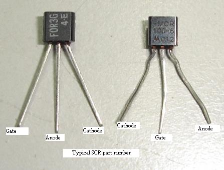
SCR...


SYMBOLS:-


OPERATION:-

An SCR is a type of rectifier, controlled by a logic gate signal. It is a four-layer, three-terminal device. A p-type layer acts as an anode and an n-type layer as a cathode; the p-type layer closer to the n-type (cathode) acts as a gate. It is unidirectional in nature.

CONSTRUCTION OF SCR:-

It consists of a four layers pellet of P and N type semiconductor materials. Silicon is used as the intrinsic semiconductor to which the proper impurities are added. The junctions are either diffused or alloyed. The Planar construction is used for low power SCR's, here all the junctions are diffused. The Mesa type construction is used for high power SCR's. In this case junction J2 is obtained by diffusion method and then the outer two layers are alloyed to it because the PNPN pellet is required to handle large currents. It is properly braced with tungsten or molybdenum plates to provide greater mechanical strength. One of these plates is hard soldered to a copper stud, which is threaded for attachment of heat sink. The doping of PNPN will depend on the application of SCR.

MODES OF OPERATION:-

In the normal "off" state, the device restricts current to the leakage current. When the gate-to-cathode voltage exceeds a certain threshold, the device turns "on" and conducts current. The device will remain in the "on" state even after gate current is removed so long as current through the device remains above the holding coupling. Once current falls below the holding current for an appropriate period of time, the device will switch "off". If the gate is pulsed and the current through the device is below the holding current, the device will remain in the "off" state.

If the applied voltage increases rapidly enough, capacitive coupling may induce enough charge into the gate to trigger the device into the "on" state; this is referred to as "dv/dt triggering." This is usually prevented by limiting the rate of voltage rise across the device, perhaps by using asnubber. "dv/dt triggering" may not switch the SCR into full conduction rapidly and the partially-triggered SCR may dissipate more power than is usual, possibly harming the device.

SCRs can also be triggered by increasing the forward voltage beyond their rated break down voltage (also called as break ver voltage), but again, this does not rapidly switch the entire device into conduction and so may be harmful so this mode of operation is also usually avoided. Also, the actual breakdown voltage may be substantially higher than the rated breakdown voltage, so the exact trigger point will vary from device to device.

SCRs are made with voltage ratings of up to 7,500 V, and with current ratings up to 3,000 RMS amperes per device. Some of the larger ones can take over 50 kA in single-pulse operation. SCRs are used in power switching, phase control, chopper, battery charger, and inverter circuits. Industrially they are applied to produce variable DC voltages for moters (from a few to several thousand HP) from AC line voltage. They control the bulk of the dimmers used in stage lighted, and can also be used in some electric vehicles to modulate the working voltage in a jacabson circuit. Another common application is phase control circuits used with inductive loads. SCRs can also be found in welding power suplies where they are used to maintain a constant output current or voltage. Large silicon-controlled rectifier assemblies with many individual devices connected in series are used in high voltage DC converter stations.

Two SCRs in "inverse parallel" are often used in place of a TRIAC for switching inductive loads on AC circuits. Because each SCR only conducts for half of the power cycle and is reverse-biased for the other half-cycle, turn-off of the SCRs is assured. By comparison, the TRIAC is capable of conducting current in both directions and assuring that it switches "off" during the brief zero-crossing of current can be difficult.

Typical electrostatic discharge (ESD) protection structures in integrated circuits produce a parasitic SCR. This SCR is undesired; if it is triggered by accident, the IC can go into latch up and potentially be destroyed.


September 20, 2009

Transistor codes..

NPN transistors
CodeStructureCase
style
IC
max.
VCE
max.
hFE
min.
Ptot
max.
Category
(typical use)
Possible
substitutes
BC107NPNTO18100mA45V110300mWAudio, low powerBC182 BC547
BC108NPNTO18100mA20V110300mWGeneral purpose, low powerBC108C BC183 BC548
BC108CNPNTO18100mA20V420600mWGeneral purpose, low power
BC109NPNTO18200mA20V200300mWAudio (low noise), low powerBC184 BC549
BC182NPNTO92C100mA50V100350mWGeneral purpose, low powerBC107 BC182L
BC182LNPNTO92A100mA50V100350mWGeneral purpose, low powerBC107 BC182
BC547BNPNTO92C100mA45V200500mWAudio, low powerBC107B
BC548BNPNTO92C100mA30V220500mWGeneral purpose, low powerBC108B
BC549BNPNTO92C100mA30V240625mWAudio (low noise), low powerBC109
2N3053NPNTO39700mA40V50500mWGeneral purpose, low powerBFY51
BFY51NPNTO391A30V40800mWGeneral purpose, medium powerBC639
BC639NPNTO92A1A80V40800mWGeneral purpose, medium powerBFY51
TIP29ANPNTO2201A60V4030WGeneral purpose, high power
TIP31ANPNTO2203A60V1040WGeneral purpose, high powerTIP31C TIP41A
TIP31CNPNTO2203A100V1040WGeneral purpose, high powerTIP31A TIP41A
TIP41ANPNTO2206A60V1565WGeneral purpose, high power
2N3055NPNTO315A60V20117WGeneral purpose, high power
Please note: the data in this table was compiled from several sources which are not entirely consistent! Most of the discrepancies are minor, but please consult information from your supplier if you require precise data.
PNP transistors
CodeStructureCase
style
IC
max.
VCE
max.
hFE
min.
Ptot
max.
Category
(typical use)
Possible
substitutes
BC177PNPTO18100mA45V125300mWAudio, low powerBC477
BC178PNPTO18200mA25V120600mWGeneral purpose, low powerBC478
BC179PNPTO18200mA20V180600mWAudio (low noise), low power
BC477PNPTO18150mA80V125360mWAudio, low powerBC177
BC478PNPTO18150mA40V125360mWGeneral purpose, low powerBC178
TIP32APNPTO2203A60V2540WGeneral purpose, high powerTIP32C
TIP32CPNPTO2203A100V1040WGeneral purpose, high powerTIP32A
Please note: the data in this table was compiled from several sources which are not entirely consistent! Most of the discrepancies are minor, but please consult information from your supplier if you require precise data.

Field Effect transister (FET)

Introduction:-
A field-effect transistor (FET) is a type of transister commonly used for weak-signal amplification (for example, for amplifying wireless signals).The device can amplify analog or digital signals.It can also switch DC or function as an oscillator.Field-effect transistors are fabricated onto silicon integrated circuit (IC) chips.A single IC can contain many thousands of FETs, along with other components such as resistors, capacitors, and diodes.

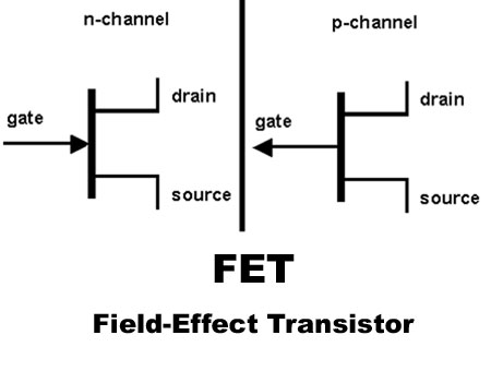
circuit symbol:-

fet-field-effect-transistor.jpg (450×340)
in real....

In the FET, current flows along a semiconductor path called the channel. At one end of the channel, there is an electrode called the source. At the other end of the channel, there is an electrode called the drain. The physical diameter of the channel is fixed, but its effective electrical diameter can be varied by the application of a voltage to a control electrode called the gate.The conductivity of the FET depends, at any given instant in time, on the electrical diameter of the channel. A small change in gate voltage can cause a large variation in the current from the source to the drain. This is how the FET amplifies signals.

Channel..
The junction FET has a channel consisting of N-type semiconductor (N-channel) or P-type semiconductor (P-channel) material; the gate is made of the opposite semiconductor type. In P-type material, electric charges are carried mainly in the form of electron deficiencies called holes. In N-type material, the charge carriers are primarily electrons.In a JFET, the junction is the boundary between the channel and the gate.Normally, this P-N junction is reverse-biased (a DC voltage is applied to it) so that no current flows between the channel and the gate.However, under some conditions there is a small current through the junction during part of the input signal cycle.

Classification:-

Field-effect transistors exist in two major classifications.These are known as the junction FET (JFET) and the metal-oxide- semiconductor FET (MOSFET).

Advantages & disadvantantages:-

The FET has some advantages and some disadvantages relative to the bipolar transister.Field-effect transistors are preferred for weak-signal work, for example in wireless communications and broadcast receivers.They are also preferred in circuits and systems requiring high impedance.The FET is not, in general, used for high-power amplification, such as is required in large wireless communications and broadcast transmitters.

DOOR BELL FOR DEAF CLICK HERE

Electronics is the study and use of electrical that operate by controlling the flow of electrons or other electrically charged particles in devices such as thermionic valves. and semiconductors. The pure study of such devices is considered as a branch of physics, while the design and construction electronic circuits to solve practical problems is called electronic engineering.

Popular article